Recently, Jieluo Intelligent Equipment (Suzhou) broke ground on its headquarters project in Wuzhong district. The site covers 42.5 mu, about 70,000 square metres of floor area, with total investment of 1.2 billion yuan. It will build a headquarters base producing 2,000 trackless-navigation robots, or AMRs, and 500 wafer smart-storage units a year. Once running, estimated annual output value is 2.5 billion yuan.
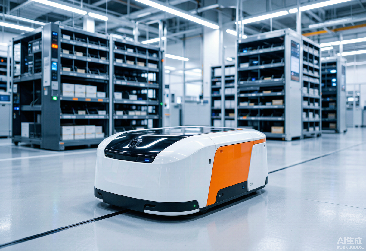
As a national little-giant specialised enterprise in semiconductor smart equipment, Jieluo rooted in Wuzhong in 2020, focusing on semiconductor AMHS overall solutions, smart mobile robots, or AMRs, and Industry 4.0 IoT systems. It serves about 70 per cent of the world’s top semiconductor chip firms and has scaled deployments at multiple domestic wafer fabs and advanced packaging plants. Since founding, it has won backing from Hefei Construction Investment, Shenzhen Capital, Huixin, SAIF, Zihe and Wuzhong Jin Kong.
Drawing on its founders’ years in semiconductors, Jieluo owns full-stack algorithm, software and hardware ability. Its 10,000 square metre plant meets ISO Class 1, the highest clean standard, and it claims a 100 per cent customer repurchase rate and zero abandoned projects.
The firm has built over ten wafer-handling AMR models and laid out wafer libraries and overhead-rail systems, forming a diverse matrix and an Industry 4.0 unmanned-factory plan. In one AI-enabled wafer-material handling scene, Jieluo’s plan cuts single-shift labour by 86.7 per cent, lifts per-robot daily handling to three times manual, raises cross-workshop efficiency by 75 per cent, shortens overall production cycles by 15 per cent and speeds new-workshop deployment by over 90 per cent. It removes manual-handling risk, drives wafer damage to zero, lifts core yield to 99.5 per cent, and holds 1,200 days of accident-free production with 100 per cent clean-room compliance.
Per February 2026 data, Jieluo’s 2025 sales doubled, with net profit of 45 to 50 million yuan. Its 2026 order book already exceeds 1.5 times full-year 2025. WSTS forecasts the 2026 global semiconductor market at 1.5 trillion US dollars, up about 90 per cent from 2025, a new high. As the industry expands and processes get finer and smarter, demands on cleanliness, precision and yield keep rising. Traditional manual handling and ordinary industrial gear lack the precision and discipline to match high-end wafer making, so upgrade pressure is acute.
Semiconductor-specific robots are the core fix. They fit ultra-clean rooms, with high precision, low dust and corrosion resistance, and can fully automate the handling, transfer and inspection of wafers and carriers, replacing risky, error-prone manual work at the source. YH Research puts the 2024 global semiconductor-robot market at 11.56 billion yuan, with steady growth to 17.04 billion yuan by 2031, a 6.0 per cent compound annual rate from 2025 to 2031.
As semiconductor processes tighten and clean standards rise, plus the push to cut cost and lift quality, semiconductor smart equipment is upgrading fast toward cleaner and more flexible forms.
Editor’s note: This is an adapted translation of the original OFweek Robotics report. It has been trimmed and restructured for readability for an international business audience.