AI data centres keep demanding more DRAM capacity and bandwidth, and memory makers are pushing harder on the next shrink path. Two of them have just chosen opposite directions in the same week.
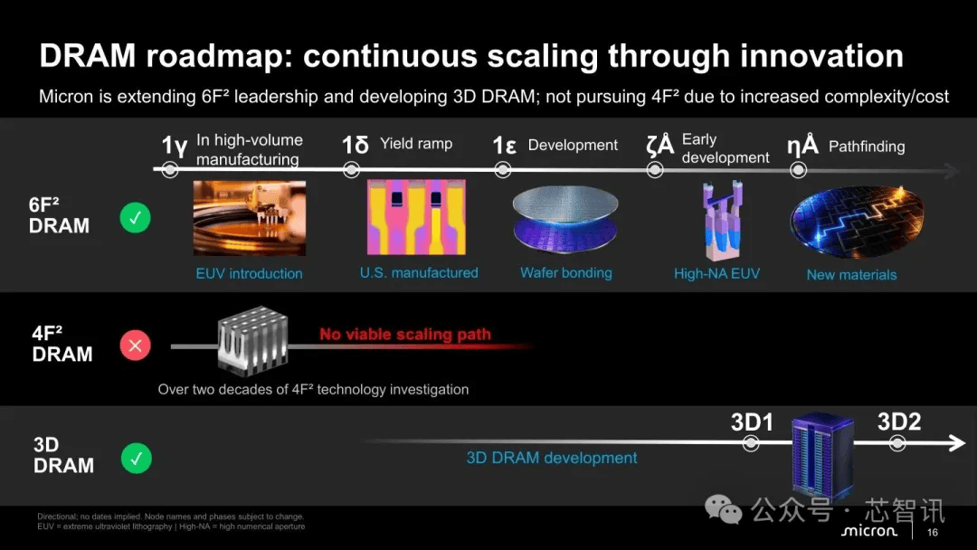
CXMT, China’s largest DRAM maker, had just announced a breakthrough in the 4F-squared architecture, with products expected before the end of 2026. Micron, the US memory major, said it will not commercialise that architecture at all. It will extend its existing 6F-squared line instead, and put wafer bonding and 3D DRAM on the roadmap.
The 4F-squared case
A conventional DRAM cell is one transistor and one capacitor, the familiar 1T1C structure. As processes shrink, cell area keeps falling, but electrical interference between transistors, leakage control, process complexity and the need to hold enough charge in the capacitor all make further scaling harder.
In a 6F-squared layout a cell occupies 6F squared of theoretical area. The 4F-squared architecture tries to cut that to 4F squared, where F is the minimum feature size tied to cell layout. On paper that is a reduction of about one third. All else equal, more cells fit per unit area, and density rises.
Getting there usually requires structural innovation such as vertical channel transistors, rearranging how transistors and interconnects sit inside the cell. Samsung Electronics and SK Hynix have both published work on the approach, hoping to extend the 10-nanometre class DRAM shrink.
CXMT has now said its own 4F-squared work has progressed, and that it plans to launch server DDR5 RDIMM products on the architecture before the end of 2026. It is using vertical gate-all-around transistors and similar techniques to control leakage and push 4F-squared toward a product.
Theoretical area advantage does not guarantee real density, performance or cost. 4F-squared has to clear transistor control, bit line coupling noise, process integration and yield. At advanced nodes, every added process step can erode cost competitiveness.
Micron’s argument: the density gain was overstated
At the 21 October roadmap seminar, Scott DeBoer, Micron’s president and chief technology and product officer, gave the reason directly. Micron studied 4F-squared DRAM for twenty years and built prototypes for comparison. It chose not to proceed because of higher complexity and cost, plus limits on how much further it could be scaled.
DeBoer stressed that bit density depends heavily on the pitch, size and geometry of the storage capacitor, not simply on whether the transistor cell is laid out in 4F-squared or 6F-squared. Change the transistor layout and the capacitor is still bound by the same constraints, so overall density may not improve in line with the theoretical area reduction.
At older nodes, 4F-squared can offer real gains, at higher cost and complexity. Pushed to advanced nodes, it runs into more fundamental scaling barriers.
That does not make the architecture worthless. It means the advantage is conditional on node, device structure, capacitor design and how the whole process fits together. Micron’s call is its own technical assessment and says nothing definitive about Samsung, SK Hynix or CXMT.
What Micron does instead
The roadmap has four layers: continue node scaling, introduce wafer bonding, optimise the peripheral logic layer, and explore 3D DRAM.
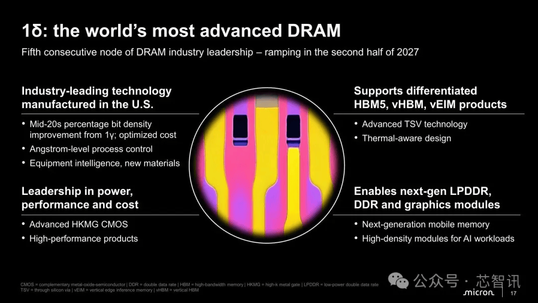
1-delta in the second half of 2027. Micron plans to ramp its seventh-generation 10-nanometre class node in Boise, Idaho, starting in the second half of 2027. DeBoer described it as the fifth consecutive node where Micron holds the industry lead and as the most advanced DRAM process in the world. It combines angstrom-scale process control with advanced high-k metal gate CMOS and new materials, and is expected to deliver roughly 20 to 30 per cent bit density improvement over the earlier 1y node.
The node is the base layer for Micron’s AI products. Through advanced through-silicon vias and thermal-aware design it supports the next generation HBM5, along with vertical HBM and vertical edge inference memory aimed at AI inference. It also feeds next-generation LPDDR, DDR and high-density graphics and memory modules built for AI workloads.
1-epsilon with wafer bonding. After 1-delta, Micron is developing a wafer-bonded node designated 1-epsilon. Bonding connects different wafers or chip layers, opening design space for device structure, peripheral circuit layout and three-dimensional integration. The value is not only smaller transistors but a rearranged relationship between the memory array and its periphery. Bonding brings its own problems: interface quality, alignment precision, thermal budget, interconnect reliability and cost.
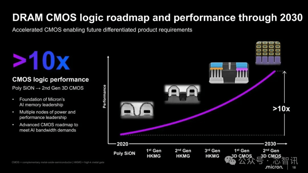
Peripheral CMOS, more than 10-fold by 2030. Micron published a roadmap for the DRAM peripheral CMOS logic layer running to 2030, projecting more than a 10-fold performance increase. The process starts from a 2020 baseline of polysilicon, passes through three generations of high-k metal gate work, and lands on first and second generation 3D CMOS structures around 2030. Micron frames this as the basis for keeping an AI memory lead, pushing DRAM logic design toward the kind of 3D chip stacking found at advanced logic foundries.
3D DRAM as a parallel track. 3D DRAM sits between the 1-zeta and 1-eta nodes in the plan, but DeBoer was careful: it is a parallel research line, not a committed replacement at a specific node. Timing will depend on maturity, product demand, cost and device performance.
The idea is vertical integration to break the area, interconnect and layout limits of a planar array. It is not stacking existing DRAM chips. DRAM still has to satisfy capacitor storage, refresh, read and write speed, signal integrity and heat dissipation, and a three-dimensional structure makes process integration harder again. Micron has given no commercial timeline.
Vertical HBM. Micron also described vertical HBM, which would integrate memory directly above the processor rather than stacking DRAM dies and packaging them next to an accelerator. Shorter data paths, higher bandwidth, deeper co-design with the processor. It is related to but distinct from 3D DRAM, which targets the array itself rather than the memory-to-processor interface. As models grow and inference workloads multiply, interconnect distance, package area and power in conventional packaging have become binding constraints.
The competitive picture
Samsung and SK Hynix have both published 4F-squared research, leaning on vertical channel transistors to extend advanced DRAM scaling. CXMT is pushing toward product. Micron has stepped off the commercial path.
Product plans, prototype validation and stable volume production are three different stages. Whether CXMT hits its end-2026 target, and whether yield, capacity, speed, reliability and unit cost meet market requirements, needs data that does not yet exist.
It is equally true that the Samsung and SK Hynix route cannot be judged from architecture names or research milestones.
4F-squared should not be read as a route that must win. What decides competitiveness is the balance across density, performance, power, yield, capital intensity and ramp speed. If 4F-squared delivers genuinely higher density at advanced nodes while keeping process complexity in check, it has commercial value. If the advantage cannot cover the extra manufacturing cost, other routes win on economics.
The DRAM industry spent decades raising density by shrinking the process and the cell area. As physical limits bite, shrinking the transistor alone no longer guarantees density gains. The capacitor, the peripheral circuits, the interconnect and the manufacturing cost have all become the binding constraints.
For Samsung, SK Hynix, Micron and CXMT alike, the challenge is not who adopts a particular architecture first. It is who can turn a technical approach into manufacturable, competitive, iterable product while AI infrastructure keeps pulling for bandwidth and capacity.
Editor’s note: This is an adapted translation of the original Sohu Tech report. It has been trimmed and restructured for readability for an international business audience. The full original (in Chinese) is at https://www.sohu.com/a/1091527502_128469.