Chip compute is scaling quickly, but memory and network bandwidth have lagged behind. The constraint is the physical limit of electrical interconnects. Researchers at MIT, the University of California Berkeley and the University of Colorado Boulder spent a decade developing the first microprocessor to communicate with memory using light signals. In 2015 they founded Ayar Labs, starting with in-package optics for high-performance computing and pivoting at the 2018 Series A to co-packaged optics, or CPO, for large-scale AI infrastructure.

Unlike early transition designs from Broadcom that assembled separate CPO modules and switch chips on one board, Ayar integrates optical engine chiplets directly into the system-on-chip. Against pluggable optics plus electrical SerDes, the company claims five to ten times the bandwidth, one tenth the latency and four to eight times the energy efficiency.
A strategic investment sweep
Ayar’s investor list reads like a roll call of the semiconductor industry. Nvidia, AMD, Intel, GlobalFoundries, MediaTek and Alchip all participated, alongside NTT DOCOMO Ventures and server maker Wiwynn. In 2026 it closed a USD 500 million Series E led by Neuberger Berman, with Alchip, ARK Invest, Insight Partners, MediaTek, the Qatar Investment Authority, Sequoia Global Equities and 1789 Capital joining. An additional USD 150 million followed. Earlier backers included IAG Capital Partners, Light Street Capital, Playground Global, Founders Fund and GlobalFoundries. Total funding exceeds USD 1 billion, with a valuation above USD 5 billion according to Reuters.
CPO relocates the electrical-to-optical step from a front-panel module into the same package as the GPU, ASIC or switch. A traditional path runs from the chip through 15 to 30 centimetres of copper trace to a front-panel module with a DSP and optical engine, then to fibre. The CPO path uses millimetres of on-package connection, an integrated optical engine and fibre. Nvidia shipped two CPO switches at GTC 2025, Quantum-X and Spectrum-X, using 1.6T and 3.2T silicon-photonics chips now entering production.
Huang did the arithmetic at the same event. A traditional GPU needs six pluggable transceivers at 30 watts each. At one million GPUs that single stage consumes about 180 megawatts, unsustainable at cluster scale. CPO shortens electrical traces from tens of centimetres to millimetres and removes the power-hungry DSP, cutting interconnect energy by more than half.
Why scale-up is the real prize
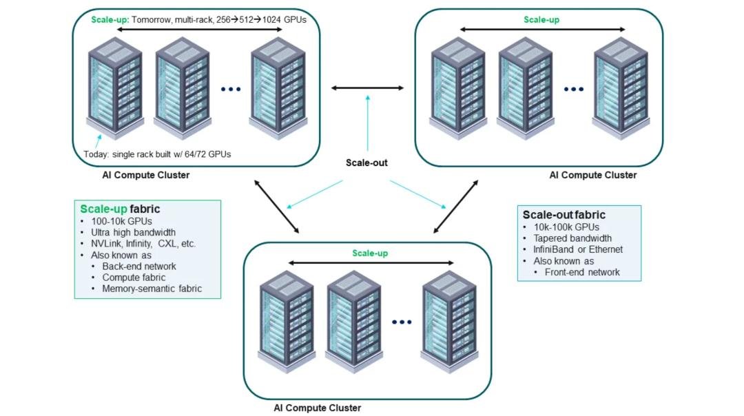
AI interconnects have two layers. Scale-out links independent nodes or racks using Ethernet or InfiniBand, already widely optical. Scale-up operates inside a node or supernode, such as a single rack of 72 GPUs, maximising bandwidth and minimising latency so chips can share memory. At 200G per lane, passive copper reaches only about two metres, confining copper-based scale-up to one or two racks. CPO can break both the bandwidth and distance limits, joining hundreds or thousands of GPUs across racks into one machine.
Ayar argues scale-up needs at least ten times the per-card bandwidth of scale-out and one tenth the latency, which requires integrating optical chiplets inside the GPU package. Its optical I/O has two parts. TeraPHY is a silicon-photonics and CMOS chiplet packaged alongside the compute die, using the UCIe interface. The current 45-nanometre generation has eight optical ports at 512 gigabits per second each, delivering four terabits per second one way and eight both ways, with ten nanoseconds of internal latency. SuperNova is an external multi-wavelength laser source that feeds 16 fibres and up to 256 data channels, supporting 16 terabits per second bidirectionally. With TSMC’s COUPE platform, a single TeraPHY engine now exceeds 13.5 terabits per second one way.
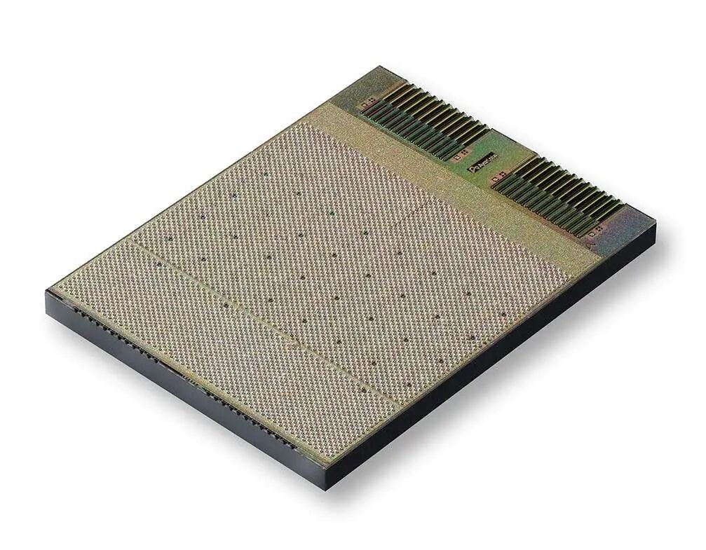
Working with Alchip and Wiwynn, Ayar built a full optical AI system. Each compute tray carries one CPU and two AI ASICs, each surrounded by eight new TeraPHY engines with hot-swappable SuperNova sources, giving a single accelerator more than 100 terabits per second of optical bandwidth. The rack uses full cold-plate liquid cooling for more than 100 kilowatts and supports maintenance without downtime. Thirty-two trays hold 64 ASICs, and sixteen racks form a scale-up cluster above 1,024 accelerators behaving like one very large GPU.
Where optical interconnect goes next
CPO commercialisation follows three steps: scale-out switches, scale-up compute chips, and optical memory extension. Between 2025 and 2026 it landed first in Nvidia and Broadcom switches, but SemiAnalysis estimates scale-out is only nine per cent of cluster power, so the saving is two to seven per cent. The larger opportunity is scale-up, where per-card bandwidth demand is nine times higher. A production inflection is expected in 2027 and 2028 as CPO enters GPU and ASIC packages and processes shift from 45-nanometre monolithic designs to 3D heterogeneous integration such as TSMC COUPE.
Creative Strategies estimates the optical interconnect market could reach USD 30 to 50 billion by 2030. Two openings remain for startups. One is decoupling compute from memory with low-latency optical links to shared pools of tens or hundreds of terabytes, since GPUs bound to HBM can usually place only eight to twelve stacks and Microsoft has disclosed that up to 25 per cent of Azure server memory sits idle. The other is acting as a neutral optical supplier for custom silicon, using open standards such as UCIe to turn optical engines into standardised chiplets. As chip giants integrate vertically, the independent layer may be the one that scales fastest.
Editor’s note: This is an adapted translation of the original 36Kr report. It has been trimmed and restructured for readability for an international business audience. The full original (in Chinese) is at https://36kr.com/p/4077867964519559.