The Chinese chip primary market is hot again. After the last domestic GPU investment round moved into payoff, capital went hunting for the next batch of AI-chip winners. The labels vary, near-memory computing, compute-in-memory, 3D near-memory, 3D TokenPU, but they keep landing under one tag: 3D stacking.
Some 3D chip firms closed two funding rounds in six months, raising close to 1 billion yuan in total. Others reached a valuation near 10 billion yuan before a single chip shipped. Yet when investors actually compared them, they found that similar technical language hid different markets, different engineering problems and different standards of commercial proof.
“The architectures all look about the same. Which product is best, and who can land the big customer, we have no idea,” one investor who backed a listed GPU company told LeiPhone. After the last cycle, his fund waits for tapeout and real orders before committing.
Why 3D stacking, and why now
Agents stretch a one-off model question into a running task. Every document checked, every judgement formed, every open question gets reassembled into the next prompt. As model calls multiply and context grows, the chip must do more compute and face a rising volume of data access.
Bringing data closer to compute is the shared story of this startup wave, and 3D stacking is the technique used to recombine chiplets, expand memory and fuse compute with storage. But stacking the same chip vertically solves different problems for different firms.
Route one: recombine the logic
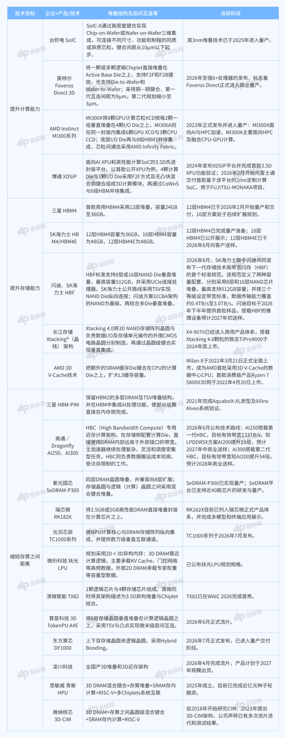
TSMC’s SoIC, Intel’s Foveros and AMD’s MI300 split and recombine logic chiplets, including compute and input-output, to keep extending performance. This route does not redefine computing. It lets chiplets of different functions and processes keep scaling together as advanced-node shrink grows expensive.

Route two: expand the memory
HBM, HBF and 3D V-Cache attack the memory problem. They pack more data into a limited package area and speed its arrival at the compute unit. They target bandwidth, capacity and cache layers respectively, but the core aim is the same, strengthen the memory supply around the compute chip.
Route three: rebuild compute next to storage
The third route changes the position of compute and storage. UNIC, Rockchip and several domestic 3D near-memory startups try to vertically integrate logic with DRAM. Samsung’s HBM-PIM, Simingwei and Winano move part of the compute onto the storage side.
Where overseas leaders use Chiplet, HBM and advanced packaging to grow system scale, domestic newcomers concentrate on vertical logic-storage integration. That is not accidental.
“Only Samsung, SK Hynix, Micron, ChangXin Memory and Yangtze Memory can truly compete in 3D memory,” said Qin Yi, an AI-chip expert. That capability sits with the few firms that own memory-wafer manufacturing. The Chiplet route also depends on mature die-to-die interconnect, software and an ecosystem.
For most domestic startups, rather than fight the IDM and foundry incumbents head on, it is smarter to reorganise existing compute and storage resources at the architecture and packaging level. With advanced process, HBM and high-end packaging constrained, 3D stacking carries a special hope: close the manufacturing gap through architecture and integration.

Bandwidth is not the product
Higher bandwidth does not automatically make a better chip. Every route must still answer one question. Do shorter data distances and higher bandwidth convert into real performance, cost and token throughput?
Many domestic 3D chips, limited by mature process, show “modest compute, high bandwidth”, which happens to fit the Decode stage that is sensitive to memory bandwidth. The real test, said analyst Cheng Yi, is whether the chip can run Decode at all on silicon, and better still validate the Attention operator inside Decode, to show high enough tokens per second.
“High bandwidth must finally cash out as token throughput,” Cheng stressed. A 3D chip’s true value is dividing labour with the GPU and cutting Decode-stage cost, not posing as a general compute replacement. He is unimpressed by startups that dress up single-point metric wins as full compute substitutes.
The engineering walls
Stacking itself brings thermal and yield trouble. Compute dies and memory dies differ in size, power and temperature distribution, so thermal cycling can cause uneven stress, warping and heat build-up. Reducing layer count is the more realistic choice now. One startup’s technical lead said 4 to 6 layers is the practical range for logic-on-memory hetero-stacking today.
Even after hardware is stacked and packaged, the software stack must relearn the new memory hierarchy. Judging a startup’s software means checking its instruction-set architecture, programming model, compiler, runtime, operator library and framework support. Without software that schedules the new structure, the theoretical edge stays on the architecture diagram.
Three gates to clear
For a 3D-chip firm still exploring, moving from roadmap to product means crossing at least three gates. Prove the target workload’s performance and cost edge on real silicon. Solve heat, warping and yield in packaging. Then reach scale delivery through software adaptation and customer validation.
Capital cannot judge a project by the “3D stacking” label alone. Recombining logic chiplets, expanding memory and rebuilding compute-in-storage answer different markets and need different proofs. But every route returns to the same question. Can higher bandwidth, shorter data distance and bolder stacking truly convert into token throughput, unit cost and customer orders?
Editor’s note: This is an adapted translation of the original LeiPhone report. It has been trimmed and restructured for readability for an international business audience.