The AI infrastructure boom pushed optics into the centre of the buildout, and the optical chip, the component that converts light into electrons and back, is priced as the next hundred-billion-renminbi market. Each step from 10G to 800G and on to 1.6T and 3.2T raises both the value per chip and the size of the market.
Two cold facts arrived while the financing wave peaked. The Federal Communications Commission’s restrictions on the optical interconnect chain have not gone away, and the regulatory risk is spreading from finished modules up to the chips. At the same time, the manufacturing barriers, capacity limits and yield curves of optical chips look less forgiving than the market assumed.
Why optics looked like a sure thing
Compute capacity roughly triples every two years, memory bandwidth grows about 1.6 times and interconnect bandwidth only about 1.4 times. That gap is the I/O wall. When several GPUs work together, data movement becomes the constraint on how much of the compute is usable, and optical interconnect, with higher bandwidth, lower latency and lower power, is the way through it.
Inside the module, the optical chip is more than 30 per cent of the bill of materials, and that share is expected to rise towards 60 per cent as speeds move to 800G, 1.6T and 3.2T. Gross margin at the high end runs between 50 and 90 per cent, well above module assembly. The global laser chip market is forecast to grow from USD 2.6 billion in 2024 to USD 22.9 billion in 2030, a compound annual rate of 44.1 per cent.
That is why the highest valuations on both the US and Chinese markets sit upstream.
The manufacturing truth
It is tempting to treat an optical chip as the photonic version of an electronic chip, and assume the same path of process shrinks will work. It does not. Optical chips are process-driven, yield-led, capital-heavy and slow. The closest analogue is silicon carbide, not logic.
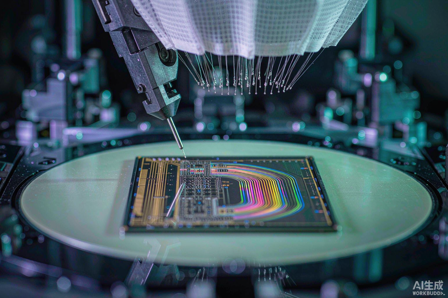
Performance comes from epitaxial structure design and growth rather than from smaller dimensions. Production covers substrate, epitaxy, wafer device fabrication and coupling and packaging. The flow is not long compared with an electronic chip, but epitaxy and grating processes need nanometre precision, the process window is narrow and yield is hard to lift.
That drives an integrated device manufacturer model, with design, fabrication and test in one company, which raises the entry barrier: heavy capital spending, a full line, and stable volume and yield. The three features of the industry follow. A complete indium phosphide line can cost several billion renminbi and depends on imported equipment with long lead times. Scale economies come from yield rather than volume, and lifting yield from 30 to 60 per cent on the same line halves the cost. Customer qualification takes about two years, from internal testing through module maker validation to end-customer approval, which makes accounts sticky and new entrants slow.
EML is the hard part
The core high-speed products are EML and continuous-wave lasers. An EML integrates a distributed feedback laser and an electro-absorption modulator on one indium phosphide die. Mask steps exceed twice those of a standard continuous-wave device and high-speed yield can fall from 50 to 15 per cent. A 200G EML is two and a half to three times as complex as a 100G part, with wafer-level yield at 10 to 20 per cent in some accounts.
Global capacity above 100G sits with Lumentum, Broadcom, Coherent and Sumitomo Electric, and Lumentum alone holds 50 to 60 per cent. Overseas yield on 100G EML runs at 75 to 85 per cent, while Chinese yield is about half that, and 200G EML at 40 to 50 per cent with most suppliers still in small batches and validation.
The constraints start with material. Indium phosphide substrate capacity is estimated at 750,000 wafers in 2026 against a shortfall above 70 per cent, and Sumitomo and AXT control 70 to 80 per cent of high-end supply. Equipment adds another gate: MOCVD tools come from Aixtron and Veeco only, order to volume takes 18 to 24 months, and a new indium phosphide line takes two to three years. Electron beam lithography for gratings runs more than a year on lead time.
Then there is the process itself, which behaves like a black box. Epitaxial growth is extremely sensitive to composition and layer thickness, and small deviations scrap a wafer. Yield climbs only through accumulated experience, which takes years.
Continuous-wave lasers are the faster-growing line and the one Chinese suppliers are pushing. They pair well with silicon photonics, and the process chain is shorter with yield easier to optimise. Domestic progress is better, with 70 milliwatt parts mature and crowded, 100 milliwatt parts still tight and likely short through 2027, and 150 milliwatt and above for near-packaged and co-packaged optics facing much higher barriers.
Customer qualification is the invisible wall. North American cloud operators set a high bar, and once a supply pattern forms it is hard to break into. A Chinese supplier that meets the technical spec still struggles to enter the mainstream North American chain quickly.
What the FCC is actually buying
The restriction is not a single cut. It is a staged squeeze by segment, designed to compress the window for Chinese substitution while American manufacturing capacity is built.
In the near term the effect is limited. Module leaders such as Innolight and Eoptolink are not on the restricted list and supply is unaffected for one to two years. Restrictions are more likely to phase in from the 3.2T generation, giving the industry two to three years of structural adjustment. Chinese suppliers hold close to 70 per cent of global 800G and 1.6T module shipments, and a painless replacement of North American supply is not available.
The long-term hit lands upstream. If the Morgan Stanley scenario applies, where about 65 per cent of the bill of materials must be US-origin to qualify for a waiver, the room for Chinese optical chips and components narrows sharply and the North American barrier rises further.
Read alongside the capacity plans, the intent is clear. Coherent is converting its Sherman, Texas plant into the first volume 6-inch indium phosphide platform, guiding to four times its wafer capacity, closely tied to Nvidia’s supply chain. Lumentum’s Greensboro site is being rebuilt as a 6-inch indium phosphide base with full ramp expected in mid-2028 for high-power EML and continuous-wave sources. Both land on the 3.2T volume window, and the policy hands them a buffer.
Two to three years, then the door
Domestic substitution in high-end optical chips only really starts in 2026. The path Chinese suppliers found is to win continuous-wave sources paired with silicon photonics first, then push into 100G and 200G EML. Several now produce 70 and 100 milliwatt continuous-wave lasers at volume and have entered leading module makers’ supply chains.
EML is a different fight. The top five overseas suppliers held about 64.8 per cent of the global laser chip market in 2025, and the highest-ranked Chinese company, Yuanjie Semiconductor, holds 3.1 per cent, concentrated in the lower and middle of the range. Some Chinese firms have 100G EML in volume, and 200G is at sampling, with global share around 4 per cent for the largest.
The window is 2026 to 2028. It exists partly because overseas leaders allocate constrained EML capacity in the order 200G, then 100G, then continuous-wave, protecting the highest-margin product first. That leaves continuous-wave open in a way it will not be later.
Silicon carbide is the reference case for what happens next. Five years ago it was the next golden sector. Within two years it went from shortage to surplus and a price collapse, with 6-inch substrate prices down 64.5 per cent and 8-inch down 79 per cent, and Wolfspeed entering restructuring after aggressive expansion into weak demand.
Optical chips are still scarce. From 2028 the market should split: oversupply at the low end, continuing tightness at the high end. EML is more exposed to temporary surplus than continuous-wave because 100G faces both a generation change and silicon photonics substitution, while continuous-wave risks a low-end glut as Chinese entrants crowd in.
The long-term risk is that the largest market stays closed. Without volume customers, Chinese suppliers cannot climb the yield curve, and a high-end chip that works but never ships in volume has no economic value.
The contest is no longer a war of endurance. It is a race with a closing door, and the sector has two to three years to stop being one or two generations behind.
Editor’s note: This is an adapted translation of the original Sohu Tech report. It has been trimmed and restructured for readability for an international business audience. The full original (in Chinese) is at https://www.sohu.com/a/1092742151_120804047.