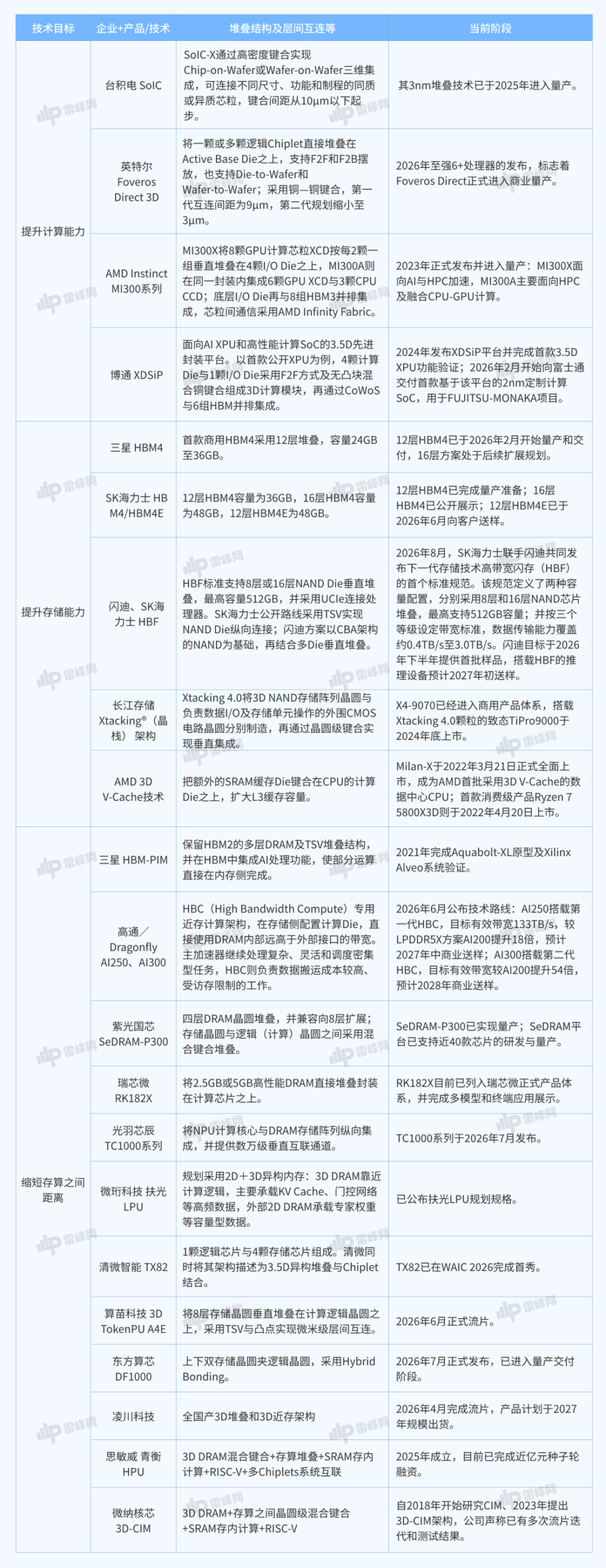
A new wave of chip funding is clustering under one label, “3D stacking”, but the companies behind it are solving three different problems. Near-memory computing, compute-in-memory and 3D near-memory sound alike and some have raised about 1 billion yuan across two rounds, yet their markets and proof points diverge.
The first route recombines logic chiplets, TSMC SoIC, Intel Foveros and AMD MI300, to keep extending performance as advanced nodes get expensive. The second expands memory, HBM, HBF and 3D V-Cache, to push more data closer to the compute. The third moves compute and storage vertically, Tsinghua, Rockchip and Samsung HBM-PIM stacking logic with DRAM.
Domestic startups lean hardest into logic-storage vertical integration, often on mature 7nm-class nodes, because advanced process, HBM and high-end packaging are constrained. The hope is that architecture and packaging close the gap left by manufacturing. Analysts note 4 to 6 stacked layers are the realistic engineering range today.
The common sales pitch is bandwidth, but the test is throughput. As one investor put it, high bandwidth must convert to tokens per second. A 3D chip only matters if it splits inference decode cheaply alongside the GPU, not if it simply posts a bigger spec sheet.
Three gates remain before any of this becomes a product: prove performance and cost on real silicon, solve heat, warp and yield in packaging, then earn software and customer validation at scale. The label sells the round. The token throughput sells the chip.
Editor’s note: This is an adapted translation of the original Leiphone report. It has been trimmed and restructured for readability for an international business audience.