A supplier of production-line equipment for two-dimensional semiconductors has closed a angel round worth tens of millions of yuan, in a bet that the next generation of chips will need a different manufacturing toolkit.
Jiyuan Technology covers the full growth, transfer and inspection chain for two-dimensional semiconductor integrated circuits. Zhaohui Xinhua Fund led the round, which is co-managed by Zhaohui Capital and Dr Zhang Rujing, the founder of SMIC. Ningchuang Tou, Changzhou High-Tech Investment and Nanhui Venture Capital joined, with Yunxiu Capital acting as financial adviser for later financing.
Founded in 2021, Jiyuan is among the earliest companies worldwide working to industrialise equipment and materials for two-dimensional semiconductors. Founder Wang Di holds an optics doctorate from the Anhui Institute of Optics and Fine Mechanics at the Chinese Academy of Sciences, was an associate researcher at Nanjing University’s National Laboratory of Solid State Microstructures, and has 15 years in two-dimensional material growth and optical inspection. He invented visual CVD technology and has experience bringing front-end inspection equipment to market.
Why silicon tools do not simply carry over
As silicon chip features approach physical limits, new materials are being tested to keep performance climbing. Two-dimensional semiconductors, only atoms thick with distinctive electrical and optical properties, are a leading candidate. But moving from lab samples to volume production takes more than a materials breakthrough. It needs a dedicated equipment set tuned to the material’s physics.
Two-dimensional materials must first be grown on sapphire or quartz substrates, then transferred to silicon through a dedicated process before chip fabrication begins. Wang says about 70 per cent of the equipment can be reused from existing silicon lines. The remaining 30 per cent has to be redesigned for two-dimensional materials, chiefly growth, special transfer and inspection.
Material transfer is the step that most separates two-dimensional manufacturing from silicon. Labs already had transfer tools, but no complete line equipment meeting mass-production requirements. Closing that gap while holding stability, process consistency, automation and throughput is the problem standing between research and a factory.
Jiyuan says it designed the world’s first wafer transfer production-line tool for two-dimensional semiconductors. It also builds growth equipment and chip inspection systems, forming a portfolio across the critical steps of integrated circuit manufacturing.
From lab instruments to line-ready tools
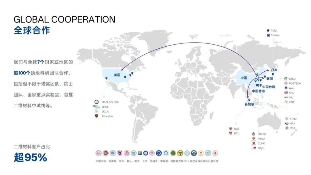
For material growth, the company developed a high-temperature in-situ optical observation CVD system. Conventional tools inspect material after the process ends. Jiyuan’s system observes and runs spectroscopy during high-temperature synthesis, giving researchers data on growth and defect formation. The company says it is the only commercially available system of its kind and has delivered more than 100 units to universities and institutes across seven countries and regions.
Wang draws a sharp line between research instruments and production-grade semiconductor equipment. Instruments serve diverse basic research needs. Line equipment must also meet the stringent standards of integrated circuit manufacturing, a distinction Jiyuan sees as its advantage over pure instrument makers.
Asked what sets the company apart, Wang points to understanding the material itself. Traditional equipment firms are engineering teams built around silicon and its processes. They may lack depth in how two-dimensional materials grow, transfer and inspect. Tool design should start from the material’s properties, then set the process and structure, rather than retrofitting silicon machines. Jiyuan’s team combines more than a decade of two-dimensional materials research with equipment industrialisation experience.
A second business in AI for science
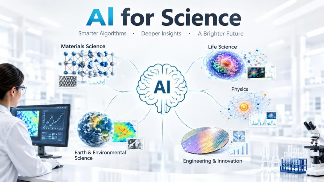
Beyond equipment, Jiyuan is extending into AI for science. It is building a platform to collect in-situ multimodal data during material synthesis and developing an agent system for materials research. It has accumulated a terabyte-scale database of high-temperature in-situ synthesis. Analysing that data lets the system identify products, locate defects, judge growth state and generate synthesis reports on its own. The next step is training agents for materials research and exploring automation in wet laboratories.
Editor’s note: This is an adapted translation of the original 36Kr report. It has been trimmed and restructured for readability for an international business audience. The full original (in Chinese) is at https://36kr.com/p/4077431786968198.